List of members |
Facilities |
Internships and jobs |
PhD |
Publications |
News |
Team
- Permanent member: Paola Atkinson
- Post-doc: Kimon Moratis
Self-assembled quantum dots, which are clusters of tens of thousands of atoms embedded in a larger bandgap material, are attractive building blocks for quantum technologies because they identify as “artificial atoms“. (See figure 1)
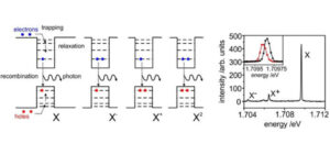
Figure 1: (left) schematic of the energy levels and carrier occupation of a QD corresponding to the neutral (X) and charged (X- and X+) excitons and the biexciton (X2); (right) low-temperature photoluminescence spectrum of a single GaAs QD showing the neutral and charged excitons (inset: zoom-in of the neutral exciton emission for two orthogonal emission polarisations showing the fine-structure splitting of the neutral exciton related to shape anisotropy of the QD).
Here we are interested in the growth of two different quantum dot systems and their integration into charge-tunable devices and photonic cavity structures for quantum optics experiments.
- GaAs / AlGaAs quantum dots. These dots are created by in situ droplet etching of nanoholes and subsequent nanohole infilling (see figure 2). This system has the advantage that the density, dot anisotropy and dot emission wavelength can all be independently controlled since each property is determined at a different stage of growth i.e. by the droplet deposition, droplet etching. and hole infilling respectively . In addition, negligible intermixing between GaAs and AlAs under the growth conditions used, together with the small difference in GaAs and AlAs lattice parameters (~0,15%) means that the dots are virtually strain free and the confinement potential can be well described by the surface morphology, facilitating modelling of the excitonic states
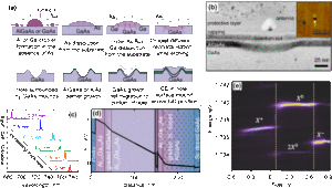
Figure 2: (a) schematic showing the stages involved in the fabrication of strain-free quantum dots: (top line) droplet deposition, substrate etching of small nanoholes (typically ~10 nm deep, 50-100 nm wide) due to dissolution of As and then Ga from the substrate into the metal droplet and final recrystallisation of the remaining droplet material to create mounds around the nanohole;, (bottom line) QD growth by preferential infilling of the self-assembled nanohole. (b) TEM measurement of a QD fabricated by droplet etching and nanohole infilling with a self-aligned plasmonic antenna above the QD (inset: AFM image of a nanohole prior to infilling) [6], (c) PL spectra of QD ensembles filled with different nominal GaAs thicknesses demonstrating that the emission wavelength can be simply controlled by the nominal thickness of GaAs deposited (spectra offset vertically for clarity) [5]. (d),(e ) Conduction band profile (d) and photoluminescence map under applied field (e) of an n-i-schottky diode structure demonstrating charge-control of the exciton emission from a single GaAs/AlAs QD [1].
- Site-controlled InAs / GaAs quantum dots. These dots are grown by the strain-driven Stranski-Krastanov growth mode due to the 7% lattice mismatch between In As and GaAs. We use substrate pre-patterning to determine the initial nucleation site of the quantum dots (see Figure 3). The advantage of this technique is that we can create ordered arrays of quantum dots, to allow the positioning of single quantum dots into arrays of photonic cavity structures for on-chip integration of quantum optics experiments.
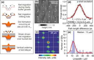
Figure 3: (a) schematic of site-controlled dot formation on a pit-patterned substrate; (b) AFM image of an ordered array of single QD (> 60% single dot occupancy) (c) PL map of the emission from an ordered array of dot bilayers (emission from the top dot layer), [4] (d) coherence lifetime measurement of a site-controlled QD 22 nm from the regrowth interface,[4] (e) histogram of the linewidths of site- controlled QDs situated 22 nm from the regrowth interface, showing the current state-of-the-art for MBE grown site-controlled QD [4].
Collaborations
- Richard Hostein, Benoît Eble, Valia Voliotis (PMTeQ, INSP)
Recent publications
- S. Germanis, P. Atkinson, R. Hostein, F. Margaillan, V. Voliotis, B. Eble, Electrical control of optically pumped electron spin in a single GaAs/AlAs quantum dot fabricated by nanohole infilling, Physical Review B 102, 035406 (2020). https://hal.archives-ouvertes.fr/hal-02891496
- S. Germanis, P. Atkinson, R. Hostein, C. Gourdon, V. Voliotis, A. Lemaitre, M. Bernard, F. Margaillan, S. Majrab, B. Eble, Dark-bright exciton coupling in asymmetric quantum dots, Physical Review B 98, 155303 (2018) https://hal.archives-ouvertes.fr/hal-01902613
- M. Pfeiffer, P. Atkinson, A. Rastelli, O. G. Schmidt, H. Giessen, M. Lippitz and K. Lindfors, Coupling a single solid-state quantum emitter to an array of resonant plasmonic antennas, Scientific Reports, 8 3415 (2018) https://hal.archives-ouvertes.fr/hal-01727540v1
- K. D. Jöns, P. Atkinson, M. Müller, M. Heldmaier, S. M. Ulrich, O. G. Schmidt and P. Michler, Triggered Indistinguishable Single Photons with Narrow Line Widths from Site-Controlled Quantum Dots Nano Letters 13, 126 (2013) http://dx.doi.org/10.1021/nl303668z
- P. Atkinson, E. Zallo and O. G. Schmidt, Independent wavelength and density control of uniform GaAs/AlGaAs quantum dots grown by infilling self-assembled nanoholes, J. Appl. Phys. 112, 054303 (2012) http://dx.doi.org/10.1063/1.4748183
- M. Pfeiffer, K. Lindfors, H. Y. Zhang, B. Fenk, F. Phillipp, P. Atkinson, A. Rastelli, O. G. Schmidt, H. Giessen and M. Lippitz, Eleven Nanometer Alignment Precision of a Plasmonic Nanoantenna with a Self-Assembled GaAs Quantum Dot, Nano Letters 14, 197 (2014) https://arxiv.org/abs/1801.03448