List of members |
Facilities |
Internships and jobs |
PhD |
Publications |
News |
Team
- Permanent members: Mahmoud Eddrief, Paola Atkinson, Jean-Eudes Duvauchelle, Franck Vidal, Masimiliano Marangolo
Using molecular beam epitaxy systems dedicated to the growth of selenide or arsenide materials respectively, we are interested in the growth of 2D materials and 2D electron gases. These are then investigated by a large variety of techniques – both structural (TEM, STM, XRD) , and electronic (ARPES, Raman spectroscopy, low temperature magneto-transport measurements…).
We are equipped with 2 MBE systems for the growth of selenides, interconnected by an ultra-high vacuum MECA2000 transfer tunnel: a RIBER 2300 machine (installed 1988) and an SVTA MBE machine (installed 2019) acquired thanks to a regional Ile-de-France equipement grant. For arsenide growth, we are equipped with a stand-alone Riber C21 machine (installed 2009), which was acquired with funding from an ANR- Emerging technologies grant.
The following lines of research are currently being explored:
- Growth of the 3D topological insulator Bi2Se3
3D Topological insulators (TI) are a relatively new class of material, characterised by a bulk energy gap and metallic surface states. These surface states, which result from a band inversion due to large spin-orbit interaction in these materials, are spin-momentum locked and topologically protected from backscattering, opening up the potential for creating dissipationless spin-polarized currents with applications in the fields of spintronics and quantum computation. Of the 3D TI materials Bi2Se3 is one of the most attractive due to its large band-gap (approx 0.3 eV) which opens up the possibility of creating TI spintronic devices operating at room temperature.
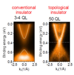
Figure 1: Transition from a conventional insulator to a topological insulator upon thickness increase as measured by ARPES on MBE-grown Bi2Se3 epilayers. (1)
However, intrinsic bulk defects result in a significant bulk carrier density and the presence of interface defects can lead to band bending and accumulation layers at the surface. These parallel conducting layers can prevent a clear signature of the surface states being visible in electrical measurements. One of the challenges for MBE growth is to reduce the bulk and interface defects in this material, both by choice of growth conditions, alloying, compensation doping, and heterostructure design. Another challenge is to create a magnetically doped TI. Of interest here is the fact that many magnetic impurities segregate, forming clusters of a different material inside the TI thin film [3].
- Growth of van-der-Waals 2D semiconductors such as GaSe
The MBE growth of GaSe on graphene with thicknesses down to 1TL has been achieved. This has permitted the significant change in band-gap and bandstructure upon reduction of the thickness from three to two to a single tetralayer of GaSeto be quantified.
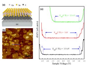
Figure 2: (a) Sketch of 1 TL GaSe on bilayer epitaxial graphene on SiC (b) STM image (300 nm x 300 nm) showing a GaSe flake containing 1TL, 2TL and 3TL thickness (c) dI/dV data showing the band-gap decrease with increasing thickness. Dashed blue lines show the valence band and conduction band edges.
- Growth of high mobility 2D electron gases by modulation doping GaAs/AlGaAs heterostructures
Using a Riber compact 21 system equipped with a single 400L/s ion pump we have grown 2DEGs with mobility of 2.106 cm2V-1s-1 for a carrier density of 3.1011 cm-2 where the 2DEG is located at a normal GaAs/Al0.33Ga0.67As interface 90 nm below the surface (see figure). This indicates that the background impurity concentration in the chamber is relatively low – in the mid 10-14 cm-3 range. We are currently investigating the growth of coupled self-assembled QD-2DEG structures for quantum information applications.
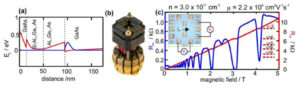
Figure 3: (a) Conduction band profile (red line) and electron wavefunction (blue line) of a modulation doped GaAs/AlGaAs heterostructure, (b) modififed PPMS (Physical Properties Measurement System) puck to accept a 20 pin LCC holder , (c) magnetotransport measurement at 2K of a 2DEG located 90 nm below the surface, inset: optical microscopy image of Hall bar used for the measurement.
Recent publications
[1] F. Vidal, M. Eddrief, B. Rache Salles, I. Vobornik, E. Velez-Fort, G. Panaccione, and M. Marangolo, Photon energy dependence of circular dichroism in angle-resolved photoemission spectroscopy of Bi2Se3 Dirac states, Phys. Rev. B 88, 241410(R) (2013). https://hal.archives-ouvertes.fr/hal-01240526/
[2] M. Eddrief, P. Atkinson, V. Etgens, B. Jusserand, Low-temperature Raman fingerprints for few-quintuple layer topological insulator Bi2Se3 films epitaxied on GaAs, Nanotechnology 25, 245701 (2014). https://hal.archives-ouvertes.fr/hal-01229143
[3] H. M. N. Vasconcelos, M. Eddrief, Y. Zheng, D. Demaille, S. Hidki, E. Fonda, A. Novikova, J. Fujii, P. Torelli, B. RacheSalles, I. Vobornik, G. Panaccione, A. J. A de Oliveira, M. Marangolo, and F. Vidal, Magnetically Hard Fe3Se4 Embedded in Bi2Se3 Topological Insulator Thin Films Grown by Molecular Beam Epitaxy, ACS Nano, 10, 1132 (2016). https://hal.archives-ouvertes.fr/hal-01366827
[4] Z. Ben Aziza, D. Pierucci, H. Henck, M. G. Silly, C. David, M. Yoon, F. Sirotti, K. Xiao, M. Eddrief, J.-C. Girard, and A. Ouerghi, Tunable quasiparticle band gap in few-layer GaSe/graphene van der Waals heterostructures, Phys. Rev. B 96, 035407 (2017). https://hal.archives-ouvertes.fr/hal-01366827
[5] A. Assouline, C. Feuillet-Palma, N. Bergeal, T. Zhang, A. Mottaghizadeh, A. Zimmers, E. Lhuillier, M. Eddrief, P. Atkinson, M. Aprili, H. Aubin, Spin-Orbit induced phase-shift in Bi2Se3 Josephson junctions, Nature Communications 10, 126 (2019). https://hal.archives-ouvertes.fr/hal-01983043