Team
- Permanent members: Romain Bernard, Yves Borensztein, Hervé Cruguel, Geoffroy Prévot, Sébastien Royer
2D-Xenes (where X = Si, Ge, Sn…) are a class of two-dimensional materials from the group IVA that possess electronic properties different from those of the corresponding 3D bulk. Calculations have shown that silicene and germanene, i.e. Si or Ge atoms arranged in a honeycomb structure, could possibly exist and display electronic, transport or magnetic properties similar to graphene’s one. With the prospect of device engineering, silicene and germanene present a better compatibility with silicon-based microelectronics. Moreover, the spin-orbit coupling leads to the opening of a small band gap (a few meV) for these materials. However, contrary to graphene, there is no layered material from which 2D-Xenes could be exfoliated. Thus, intensive research has been made in order to synthesize these 2D materials while trying to maintain their intrinsic properties.
At the Institute of NanoSciences of Paris, we study the structure and growth mechanisms of silicene and germanene obtained by material evaporation under UHV on various substrates (Ag, Al, layered materials). We use in-situ scanning tunneling microscopy (STM) and grazing incidence X-ray diffraction (GIXD) together with density functional theory (DFT) calculations in collaboration.
- Structure of silicon nanoribbons on Ag(110)
- Structure of silicene reconstructions on Ag(111)
- Silicene thin films: are they silicene?
- Growth mecanisms of silicene layers and silicon films on Ag(111)
- Optical investigation of 2D layers of Si and of silicene
1. Structure of silicon nanoribbons on Ag(110)
Because of its immiscibility with Si , Ag appears as a good candidate for the growth of a silicene layer. The first hypothesis that silicene may exist was given for silicon nanoribbons that form on a Ag(110) surface. However, the assumption that the observed structures (see Fig. 1) were actually silicon hexagons was highly controversial.
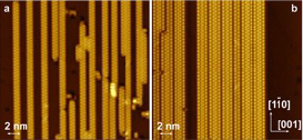
Figure 1: STM images of nanoribbons grown on Ag(110) upon Si deposition at (a) room temperature and (b) 460 K.
For the first time, we have followed, by STM imaging, the evolution of a well defined region of the sample during the growth process. Our results clearly show an important modification of the substrate during the growth. Indeed, STM images recorded during the deposition of Si show the growth of new Ag islands, either on the step edges or on the terraces (see figure 2). This implies that the adsorption of Si atoms induces the release of Ag atoms from the substrate.
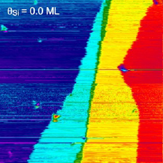
Figure 2: sequence of STM images (330 × 310 nm2) of the same area showing the evolution of the silver surface, at room temperature, upon increasing Si coverage θSi.
This result was confirmed by the evolution of the GIXD pattern during the growth, showing the formation of a missing-row reconstruction. From a direct comparison between X-ray measurements and DFT calculation, we have concluded that the Si atoms in the ribbons were arranged in rows of alternate pentamers (see figure 3). This model also agrees with STM images.
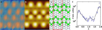
Figure 3: a) detailed STM view of a Si nanoribbon. (b) simulated STM image from DFT computation. c) model of Si pentamers (green). The red rectangle corresponds to the surface unit cell. d) comparison between experimental (blue) and simulated (black) structure factors obtained from X-ray intensities.
2. Structure of silicene reconstructions on Ag(111)
Evaporation of one monolayer (1 ML) of silicon on Ag(111) leads to the formation of various superstructures on the substrate. The most studied one corresponds to a (4×4) reconstruction with respect to Ag(111). On the basis of angle resolved photoemission spectroscopy (ARPES), STM and DFT calculations, it has been described as a (3×3) silicene reconstruction, giving rise to Dirac cones in the electronic structure near the Fermi level. We have precisely measured the diffracted intensities for this structure and we have compared the results to simulated intensities from DFT computations. A perfect agreement is found with a model of a buckled silicene layer (see figure 4). The results also indicates that the Ag substrate is relaxed upon Si adsorption, which indicates a non-negligible coupling between silicene and silver. Similar observations are obtained for the other reconstructions observed (2V3x2V3R30°) and (V13xV13R13.9°).
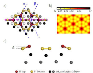
Figure 4: Top (a) and lateral (c) view of the relaxed (4×4) structure on Ag(111) computed from DFT. The two Ag bottom layers have been omitted. a and b are the angles indicated by dotted blue lines. The lateral view is a cut along the pink dotted line drawn in (a). b) Simulated STM image for a bias voltage U=2 V.
3. Silicene thin films : are they silicene?
The strong interaction between silicene and Ag modify the interesting electronic properties expected for free standing silicene. That is the reason why researchers, have tried to synthesize silicene multilayers by continuous Si evaporation on Ag substrates, in analogy with graphene multilayers. When the substrate temperature is below 540 K, a quasi layer by layer growth mode is observed, together with linear dispersion bands in the electronic structure, that cross the Fermi level near the K point. This could be the signature of Dirac cones.
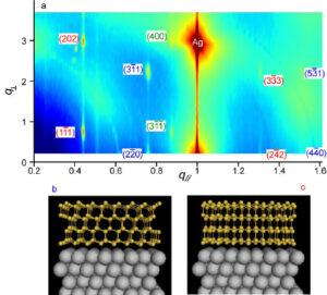
Figure 5: a) Map of the intensity diffracted by 8 ML Si evaporated on Ag(111) at T = 520K, as a function of momentum transfer parallel or perpendicular to the surface (in reduced units). The spots and rod at q//=1 correspond to the Ag substrate. The other spots correspond to the silicon diamondlike film with various orientations such as the one shown in b) and c) for 4 ML Si.
Using GIXD, we have studied the structure of 8ML Si films grown at 500 K on Ag(111). Our results unambiguously demonstrate that these films have silicon bulk structure with a (111) surface and different in-plane orientations. Moreover, we were able to measure the X-ray intensities associated with the (V3xV3) reconstruction of the silicon film. Results are well fitted with the honeycomb-chained-triangle model of Ag/Si(111). This shows that Ag atoms wet the surface of the Si films. From this study we could conclude that the linear dispersion bands cannot be attributed to silicene multilayers.
4. Growth mecanisms of silicene layers and silicon films on Ag(111)
Figure 6: sequence of STM images of the Ag(111) surface upon Si deposition at T = 500 K.
Figure 6 shows a sequence of STM images of a Ag(111) surface acquired continuously during silicon evaporation at a substrate temperature T=500 K. As soon as evaporation starts, the Ag steps, initially curved, become straight. Darker domains with triangular shapes form on the terraces, and new terraces develop. This can be interpreted as the formation of silicene domains inside the Ag terraces, growing by expelling Ag atoms that recondense at the step edges. This is in good agreement with DFT calculations showing that the insersion of a Si atom in the Ag surface is energetically favored, by 0.8 eV.
Beyond one monolayer coverage, we could also observe the transition between a silicene layer and the silicon film. This is illustrated on figure 7. The silicene layer (in blue) is progressively replaced by a thicker film covered with Ag (in green). Surprisingly, the silicon film forms by insertion of Si atoms that dislodge the atoms of the outermost Ag layer. Part of the released Ag atoms wet the Si film, while the remainder intercalate below the silicene layer.
Figure 7: comparison between two STM images of the exact same sample area for increasing Si coverage, and model for the growth of Si films.
Beyond evidencing these unexpected growth mechanisms, we understand now why it is possible to grow silicene on Ag(111), although silicon is the most stable structure for Si atoms. The energy barrier associated with the exchange of Si and Ag atoms below the silicene layer is responsible for the high stability of the silicene layer on Ag(111).
Past PhD
- Alberto Curcella (2018)
Publications
- C. Hogan, O. Pulci, P. Gori, F. Bechstedt, D. Martin, et al.. Optical properties of silicene, Si/Ag(111), and Si/Ag(110). Physical Review B: Condensed Matter and Materials Physics (1998-2015), American Physical Society, 2018, 97 (19), pp.195407. ⟨10.1103/PhysRevB.97.195407⟩. ⟨hal-01950957⟩
- Wenbing Peng, Tao Xu, Pascale Diener, Louis Biadala, Maxime Berthe, et al.. Resolving the Controversial Existence of Silicene and Germanene Nanosheets Grown on Graphite. ACS Nano, American Chemical Society, 2018, 12 (5), pp.4754-4760. ⟨10.1021/acsnano.8b01467⟩. ⟨hal-03037862v2⟩
- Alberto Curcella, Romain Bernard, Yves Borensztein, Silvia Pandolfi, Geoffroy Prévot. Transition from silicene monolayer to thin Si films on Ag(111): comparison between experimental data and Monte Carlo simulation. Beilstein Journal of Nanotechnology, Karlsruhe Institute of Technology., 2018, 9, pp.48 – 56. ⟨10.3762/bjnano.9.7⟩. ⟨hal-01701763⟩
- A. Curcella, R. Bernard, Y. Borensztein, M. Lazzeri, G. Prévôt. The mechanism for the stabilization and surfactant properties of epitaxial silicene. Nanoscale, Royal Society of Chemistry, 2018, 10 (5), pp.2291-2300. ⟨10.1039/C7NR06833F⟩. ⟨hal-01701778⟩
- Alberto Curcella, Romain Bernard, Yves Borensztein, Michele Lazzeri, Andrea Resta, et al.. Multilayer silicene: clear evidence of Ag-terminated bulk silicon. 2D Materials, IOP Publishing, 2017, 4, pp.25067 – 25067. ⟨10.1088/2053-1583/aa65b8⟩. ⟨hal-01505617⟩
- Geoffroy Prévot, Conor Hogan, Thomas Leoni, Romain Bernard, Eric Moyen, et al.. Si Nanoribbons on Ag(110) Studied by Grazing-Incidence X-Ray Diffraction, Scanning Tunneling Microscopy, and Density-Functional Theory: Evidence of a Pentamer Chain Structure. Physical Review Letters, American Physical Society, 2016, 117 (27), pp.276102. ⟨10.1103/PhysRevLett.117.276102⟩. ⟨hal-01444862⟩
- A. Curcella, R. Bernard, Y. Borensztein, A. Resta, M. Lazzeri, et al.. Determining the atomic structure of the ( 4 × 4 ) silicene layer on Ag(111) by combined grazing-incidence x-ray diffraction measurements and first-principles calculations. Physical Review B: Condensed Matter and Materials Physics (1998-2015), American Physical Society, 2016, 94 (16), pp.165438. ⟨10.1103/PhysRevB.94.165438⟩. ⟨hal-01400118⟩
- Geoffroy Prévot, Romain Bernard, Hervé Cruguel, Alberto Curcella, Michele Lazzeri, et al.. Formation of silicene on silver: Strong interaction between Ag and Si. physica status solidi (b), Wiley, 2016, 253 (2), pp.206-217. ⟨10.1002/pssb.201552524⟩. ⟨hal-01286148⟩
- Yves Borensztein, Alberto Curcella, Sébastien Royer, Geoffroy Prévot. Silicene multilayers on Ag(111) display a cubic diamondlike structure and a √ 3 × √ 3 reconstruction induced by surfactant Ag atoms. Physical Review B: Condensed Matter and Materials Physics (1998-2015), American Physical Society, 2015, 92 (15), pp.155407. ⟨10.1103/PhysRevB.92.155407⟩. ⟨hal-01400107⟩
- R. Bernard, Y. Borensztein, H. Cruguel, M. Lazzeri, Geoffroy Prévot. Growth mechanism of silicene on Ag ( 111 ) determined by scanning tunneling microscopy measurements and ab initio calculations. Physical Review B: Condensed Matter and Materials Physics (1998-2015), American Physical Society, 2015, 92 (4), pp.045415 ⟨10.1103/PhysRevB.92.045415⟩. ⟨hal-01443664⟩
- T. Leoni, Romain Bernard, A. Ranguis, Yves Borensztein, Geoffroy Prévot, et al.. Si Ultrathin Films on Silver Surfaces: An Intriguing Epitaxial System. SIGE, GE, AND RELATED COMPOUNDS 6: MATERIALS, PROCESSING, AND DEVICES, 2014, 65 S MAIN ST, PENNINGTON, NJ 08534-2839 USA, Unknown Region. pp.89-97, ⟨10.1149/06406.0089ecst⟩. ⟨hal-01238946⟩
- Geoffroy Prévot, Romain Bernard, Hervé Cruguel, Yves Borensztein. Monitoring Si growth on Ag(111) with scanning tunneling microscopy reveals that silicene structure involves silver atoms. Applied Physics Letters, American Institute of Physics, 2014, 105 (21), pp.213106. ⟨10.1063/1.4902811⟩. ⟨hal-01238949⟩
- Y. Borensztein, Geoffroy Prévot, L. Masson. Large differences in the optical properties of a single layer of Si on Ag(110) compared to silicene. Physical Review B: Condensed Matter and Materials Physics (1998-2015), American Physical Society, 2014, 89 (54), pp.245410. ⟨10.1103/PhysRevB.89.245410⟩. ⟨hal-01021106⟩
- R. Bernard, T. Leoni, A. Wilson, T. Lelaidier, H. Sahaf, et al.. Growth of Si ultrathin films on silver surfaces: Evidence of an Ag(110) reconstruction induced by Si. Physical Review B: Condensed Matter and Materials Physics (1998-2015), American Physical Society, 2013, 88 (12), pp.121411. ⟨10.1103/PhysRevB.88.121411⟩. ⟨hal-00914746⟩
5. Optical investigation of 2D layers of Si and of silicene
Team
- Permanent members: Yves Borensztein, Geoffroy Prévot
Theoretical calculations have shown that the optical properties of free-standing silicene are similar to the ones of graphene, and are dominated by the presence of the Dirac cone at the Fermi level, around the K point, and by interband transitions around the M point.
However, the Si monolayers when grown on Ag(110) or Ag(111) are in strong interaction with the substrate, and their electronic properties are completely modified with respect to what is expected for the free-standing silicene. Consequently, the optical response is also different, and appears to be rather similar to amorphous or disordered silicon, which indicates that the Si layers are sp3 hybridized and not sp2.
Optical investigation of silicene on Ag(111) and of 2d Si layer on Ag(110)
Fig.1 shows the Surface Differential Reflectance Spectrum, measured for 0.5 and 1 Si ML grown on Ag(111), defined by DR= (RSi-RAg)/RAg, where RAg and RSi are the reflectances of the pristine Ag surface and the same surface covered by Si, respectively. The spectra are completely different to what would be expected if the Si film has got the same optical response as free-standing silicene (red curve). The experiment is correctly reproduced by DFT calculation (right) for the 4×4 silicene layer. From these data, the effective dielectric function of the silicon layer can be isolated from the optical response of Ag, and is shown in Fig.2.a. The imaginary part (red) corresponds to the optical absorption. It is very well reproduced by the DFT calculation (b). On the contrary, it is different from the dielectric function calculated for free-standing silicene (black curve in (c), and close to that of amorphous Si (red curve in (c)).
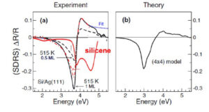
Figure 1: SDRS of Si/Ag(111): (a) Experimental measurements at 515K for 0.5 ML (dashed black line) and 1.0 ML (solid black line) and at 600K for 1.0 ML (dot-dashed red line). The continuous red line is what would be expected if the silicene layer have the same optical response as free-standing silicene. (b) Computed spectrum for the (4 × 4) model (corresponding to 1.0 ML coverage). }
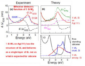
Figure 2: Surface dielectric difference (SDD) spectra of Si/Ag(111). (a) Experimental data at 515 and 600K (imaginary part only, blue dot-dashed line). (b) Computed SDD spectra for the 4 × 4 structure (solid red and black dashed curves). Also shown are the imaginary parts of the slab dielectric function for the clean (Ag: dot-dashed magenta line) and Si-covered surface (Si/Ag: green dots). (c). Imaginary part of the dielectric function of free-standing silicene, of 1 crystalline Si monolayer and of 1 amorphous Si monolayer.
In Figure 3, similar experiments has been done, using the Reflectance Anisotropy Spectroscopy, which gives the anisotropy of the reflectance along the two main direction : [001] and [1-10]. The RAS of the first layer of Si grown on Ag(110) is shown. It has been demonstrated experimentally, by X-ray diffraction in our group and by DFT calculations in collaboration with Hogan’s group in Rome, that this layer was not silicene, but instead was formed by pentamer ribbons. This is confirmed by the optical measurements shown in this figure, which are in good agreement with the DFT calculations, both for the single and double nano-ribbons made of pentamer chains, but not for another proposed model, the zig-zag model.
Figure 3: RAS of Si/Ag(110). (a) Experimental data before and after deposition of 1-ML Si nanoribbons at RT. (b) Computed spectra for the clean surface, pentamer chain model (SNR and DNR), and zigzag chain model (SNR).
Silicon multilayers grown on Ag(111) are not silicene multilayers
Optical measurements, combined with Auger electron spectroscopy and X-ray diffraction show that Si multilayers grown on Ag(111) have actually the bulk-Si (diamond-like) structure, and are covered by a thin layer of Ag which gives the well-known V3xV3-R30° reconstruction.
Surface Differential Reflectance Spectroscopy and Thermo-Reflectance Spectroscopy (TRS) have both been used and showed that a film of 2.1 nm grown at high temperature on Ag(111) display optical properties intermediate between bulk crystalline and amorphous Si, which is typical of poorly crystallized diamond-like Si.
Figure 4 shows the experimental TR spectrum for 2.1 nm Si / Ag (red). It displays transitions which are typical of the transitions measured on bulk crystalline Si and on Ag. Comparison with calculation shows that the spectrum cannot be reproduced by free-standing silicene (1) or by “silicite” (2). The features are reproduced correctly by bulk crystalline Si (4), and a mixture half amorphous (3), half crystalline Si (4) permits to reproduce almost perfectly the experimental (5).
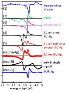
Figure 4 : Thermoreflectance spectra. Circles: experiments; red: 2.1-nm Si/Ag; black: bulk Si; blue: bulk Ag. Continuous lines: calculations for different dielectric functions of the 2.1-nm silicon film on Ag. (1): free-standing silicene; (2): “silicite”; (3): amorphous Si; (4): crystalline Si (2); (5): half amorphous/crystalline Si. For spectra (1) and (2), the dashed lines are the spectra amplified by a factor of 7. The curves have been shifted vertically for a better visualization.
Publications
- C. Hogan, O. Pulci, P. Gori, F. Bechstedt, D. Martin, et al.. Optical properties of silicene, Si/Ag(111), and Si/Ag(110). Physical Review B: Condensed Matter and Materials Physics (1998-2015), American Physical Society, 2018, 97 (19), pp.195407. ⟨10.1103/PhysRevB.97.195407⟩. ⟨hal-01950957⟩
- Yves Borensztein, Alberto Curcella, Sébastien Royer, Geoffroy Prévot. Silicene multilayers on Ag(111) display a cubic diamondlike structure and a √ 3 × √ 3 reconstruction induced by surfactant Ag atoms. Physical Review B: Condensed Matter and Materials Physics (1998-2015), American Physical Society, 2015, 92 (15), pp.155407. ⟨10.1103/PhysRevB.92.155407⟩. ⟨hal-01400107⟩
- Y. Borensztein, Geoffroy Prévot, L. Masson. Large differences in the optical properties of a single layer of Si on Ag(110) compared to silicene. Physical Review B: Condensed Matter and Materials Physics (1998-2015), American Physical Society, 2014, 89 (54), pp.245410. ⟨10.1103/PhysRevB.89.245410⟩. ⟨hal-01021106⟩