
List of members |
Facilities |
Internships and jobs |
PhD |
Publications |
News |
Team
- Permanent members: Christophe Brun, Tristan Cren, Marie d’Angelo, Pascal David, François Debontridder, Marie Hervé
- PhD Student: Hugo Le Du
- Former doctoral student: Eugenio Gambari,Axel Malécot, Ludovica Zullo
Since the discovery of topological insulators in 2007 and the emergence of topology in the field of condensed matter, new quantum phenomena have been discovered in systems that we thought we knew everything about. Like insulators, which have topological phases characterized by Dirac edge states, superconductors show topological phases with so-called Majorana edge states. One of the team’s flagship projects is to explore different ways of generating such topological superconductivity. For this we are studying superconducting systems with a very strong spin-orbit coupling which should give rise to the formation of triplet spin symmetry components of the superconducting order parameter.
We also pay particular attention to topological semi-metals which are electronic metals/semimetals with strong spin-orbite coupling. Their Fermi surfaces show crossings between conduction and valence bands, produced by a non-trivial topology and which are protected by symmetry, making them robust against external perturbations. These topological phenomena in the electronic properties of matter are of great interest due to potential applications in the field of quantum information.
- Topological superconductivity
- Dispersive Majorana states in 2D
- Pairs of Majorana bound states in a 2D system
- Topological semi-metals
The team has evidenced the existence of new “topological” quantum states, dispersive Majorana states and zero energy Majorana state pairs, in a system combining a two-dimensional superconductor and magnetic nano-structures. Numerous theoretical works predicted the existence of these new quantum states that could be useful to realize quantum computers.
Once limited to the field of fundamental mathematics, topology made a triumphant arrival in the world of physics with the discovery of topological insulators in 2007. By looking at the properties of insulators with new eyes, it became apparent that materials could be separated into different categories according to their topology: the so-called “trivial” insulators such as silicon and the so-called “topological” insulators such as Bi2Se3. Topological insulators have the remarkable property of having a metallic state on their surface while in volume they are insulating. The electronic structure of the surface states of topological insulators is similar to that of graphene (graphite monolayer) except that the electrons are entirely spin-polarized, the electrons propagating in one direction have a spin opposite to those propagating in the opposite direction. Like insulators, superconductors, those materials that conduct electricity infinitely well, are also supposed to have topological properties. Indeed, to be able to define trivial or topological properties, it is sufficient that the physical properties are described by energy bands separated by a forbidden energy band, the gap. Since superconductors have a particular electronic structure with a gap, it is therefore possible to obtain “trivial” and “topological” superconductors, the latter having to present very particular edge states: Majorana edge states. In one-dimensional systems such as topological superconducting wires, two Majorana bound states are expected to be observed in the gap, exactly at zero energy, located at the ends of the wires. In 2D and 3D systems, the Majorana states can propagate along the 1D or 2D edges, so instead of having bound states as in 1D, one expects to obtain dispersive Majorana states with an energy structure similar to that observed in topological insulators.
Dispersive Majorana states in 2D
Topological superconductivity emerges from the combination of several ingredients: conventional superconductivity combined with magnetism and spin-orbite interaction. This combination can be achieved using lead monolayers deposited on silicon and coupled with nanomagnets. The Pb monolayer provides both superconductivity and a strong spin-orbite interaction, known as Rashba. The magnetic component necessary for the appearance of Majorana particles comes from Co-Si nano clusters formed by self-organization and located under the Pb layer. Using this delicate combination of materials, the team has been able for the first time to measure edge states of topological superconductors in 2D [1].
By observing at 300 mK the samples thus prepared by tunneling microscopy, the topological structures appear in the form of thin rings signaling the boundary between two structures of different topology (Figure 1). These two topologies are caused by the magnetic field of cobalt: the superconducting Pb layer is normally trivial, but when it is in contact with a Co-Si nanomagnet it becomes topological. Theoretical calculations carried out in parallel have made it possible to reproduce the complete dispersion of these edge states and to highlight the link with the Majorana states opening the door to their possible use and manipulation in a quantum computing system.
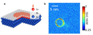
Figure 1: a.Structure of the samples studied. b. Zero energy spectroscopy revealing edge states caused by a local magnetic field due to Co atoms buried under the superconductor.
Pairs of Majorana bound states in a 2D system
As explained above, a topological superconducting wire must have two zero-energy Majorana states at each end. If instead of a wire we consider a two-dimensional topologically superconducting domain, such as a disk, it is possible to generate a pair of Majorana states through “topological” defects such as vortices or skyrmions. If only one state of Majorana is present in the center of the topological domain, a partner must appear all around the domain. It is this theoretically predicted manifestation that we have observed by directly imaging pairs of Majorana states and their zero energy spectroscopic signature [2] in the previously described system of a Pb monolayer coupled with Co-Si nanomagnets (Figure 2). Due to the nature of the technique used, we were able to visualize the spatial behavior of the Majorana pairs and their resistance to disorder. We showed that one of the Majorana states was strongly localized in the center of a magnetic island while its partner was delocalized all around the island, according to theoretical predictions.
The topological origin of Majorana excitations confers them a topological protection to low amplitude parasitic interactions. The use of these topological properties in the context of quantum information would constitute an extremely powerful tool to fight against decoherence phenomena which are currently one of the greatest challenges for the development of a quantum computer.
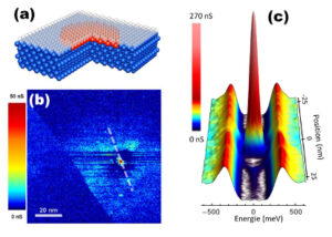
Figure 2: In (a) the studied system consists of a Pb atomic plane (in light grey) and the silicon substrate (in blue). Magnetic islands of Co-Si (in red) located under the Pb layer induce topological superconductivity locally. In (b) the topological states appear in the conductance mapping measured by scanning tunnel microscopy/spectroscopy: a red dot in the center of the topological domain is surrounded by a light blue crown on the outside of the domain. A cross-section of the measured state density across the domain is shown in (c). It can be seen that states appear at zero energy in the middle of the superconducting gap, these are the Majorana states. The large red peak corresponds to the Majorana state in the center of the domain, the very slight blue peak at zero energy corresponds to its partner located all around the domain as theoretically predicted.
Publications
- G. C. Ménard, S. Guissart, C. Brun, R. T. Leriche, M. Trif, F. Debontridder, D. Demaille, D. Roditchev, P. Simon, T. Cren.Two-dimensional topological superconductivity in Pb/Co/Si (111). Nature Communications 8, 2040 (2017) https://hal.archives-ouvertes.fr/hal-01663084
- C. Ménard, A. Mesaros, C. Brun, F. Debontridder, D. Roditchev, P. Simon & T. Cren. Isolated pairs of Majorana zero modes in a disordered superconducting lead monolayer. Nature Communications 10, 2587 (2019) https://hal.archives-ouvertes.fr/hal-03060026
Main collaborations
- We collaborate on these subjects with Pascal Simon’s team (University of Paris Saclay) for the theory.
- We are exploring new topological phases in dichalcogenides with the help of Laurent Cario’s team at IMN and Peter Samuely’s team (Slovak Academy of Science, Kosice).
Funded project
- Projet-ANR-14-CE32-0021MISTRAL (https://anr.fr/Projet-ANR-14-CE32-0021)
Recently, the team of Prof. Matsuda, one of our close collaborators at the University of Tokyo, has highlighted by angle-resolved photoemission the existence of nodal lines in Cu2Si, a two-dimensional topological semimetal. This particular electronic structure is robust to any perturbation that preserves the mirror symmetry of the system in the absence of consequent spin-orbit coupling and could lead to the development of components with novel exotic properties. However, this system, elaborated by deposition of silicon on a copper crystal has two serious disadvantages for electronic applications: the metallic substrate and the absence of gap in the electronic structure.
In a first step, we synthesized the Cu2Si layer on a semiconductor substrate by depositing copper on Si(111). Previous studies have shown that the atomic structure of the layer is identical to that of a Cu2Si layer on Cu(111). However, our results from angle resolved photoemission (ARPES) show that the electronic properties are strongly perturbed with in particular the disappearance of the nodal lines initially present around the center of the zone. DFT calculations performed by Taiwanese collaborators of the National Tsing-Hua University show that in the case of a silicon substrate, the 2D layer/substrate interactions via pz type orbitals perpendicular to the surface are too important and lead in particular to the disappearance of one of the cones at the origin of the nodal lines.
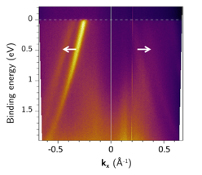
Figure 3: Doubling of electronic strips in Cu2Si, induced by lead deposition at 30eV by ARPES.
In a second step, we came back to the study of Cu2Si on a copper substrate (system thus presenting two nodal lines in its electronic structure) and we were interested in the effect of a lead deposit on the electronic properties of the 2D layer. Indeed, lead, a heavy element, is often used to induce a spin-orbite coupling effect in the surfaces on which it is deposited. In the case of Cu2Si, we have thus been able to demonstrate by XPS and ARPES that lead atoms are deposited on Si atoms on the surface and induce a doubling of the bands at the origin of the nodal lines. More recent results are still under analysis but they seem to show a gap opening in the electronic structure due to the spin-orbite coupling.
In a next step, we now plan to focus on the spin texture of the bands revealed after Pb deposition.
Main collaborator
- Yukio Tanaka (Nagoya University)