List of members |
Facilities |
Internships and jobs |
PhD |
Publications |
News |
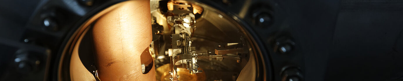
Device fabrication using clean room and air free processing in glove box
We benefit from INSP clean room, as well as access to « Paris centre clean room consortium » giving us access to optical, laser and e-beam lithography. We also have possibilities to deposit metals and dielectrics including high-k materials. In the group, we also have glove-box for air free processing of nanocrystals. This also includes an evaporator connected to the glove box for full air free fabrication of device.
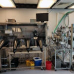
Caption: Image of setup for air free processing.
Setup for optoelectronic characterization
In addition of the facilities to fabricate the device, we also have full facilities for device characterization. This includes two close cycle cryostats, 3 probe-stations including one in air free environment, many source meters with resolution down to sub fA (Keithley 6430), current amplifier, high speed amplifier, lock in amplifier, GHz oscilloscope, many light sources from visible to mid IR, either broad band or laser source (355,405, 532, 635, 800, 940, 1550 and 4400 nm). We also have pulsed laser for time resolved experiment. We also have 3 absorption spectrometers to cover the range from 200 nm and up to 200 µm.
Contact
- Emmanuel Lhuillier : emmanuel.lhuillier(at)insp.upmc.fr