List of members |
Facilities |
Internships and jobs |
PhD |
Publications |
News |
Team
- Permanents members : Agnès Maitre, Willy Daney de Marcillac
- PhD students : Sergei Celaj, Charlie Kersuzan
- Scientist visitor: Arnaud Raoux
Emission of semiconductor nanocrystals at the individual scale
Semiconductor core/shell nanocrystals are known as colloidal quantum dots. With a characteristic size of just a few nanometers, they confine carriers (electrons and holes) to a very small volume. Energy levels are then discretized as in an atom. These quantum boxes are also known as artificial atoms.
The 2023 Nobel Prize in Chemistry was awarded to Moungi Bawendi, Louis Brus and Alexei Ekimov, for the discovery and synthesis of these quantum dots.
Their emission wavelength depends on their size. For CdSe/CdS nanocrystals, emission is in the visible range, for us essentially around 600nm in the red. On an individual scale, these nanocrystals emit photons one by one, known as single photons.
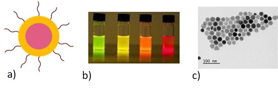
a) Schematic diagram of a colloidal quantum box. Core: CdSe; shell: CdS; outside: ligands that prevent nano-emitter aggregation. b) Fluorescence of quantum dots c) Electron microscopy image of quantum dots (Synthesis T. Pons, C. Roux-Byl, LPEM).
We work in collaboration with Thomas Pons who synthesizes them in his group (LPEM, ESPCI).
Characterization
For an individual nanocrystal, we use fluorescence microscopy to measure its spectrum, intensity and radiation pattern. We carry out lifetime and anti-coincidence measurements to verify that the nanocrystal is indeed emitting single photons. We have developed methods for determining the orientation of an individual nano-emitter as a function of its emission polarization and radiation pattern.
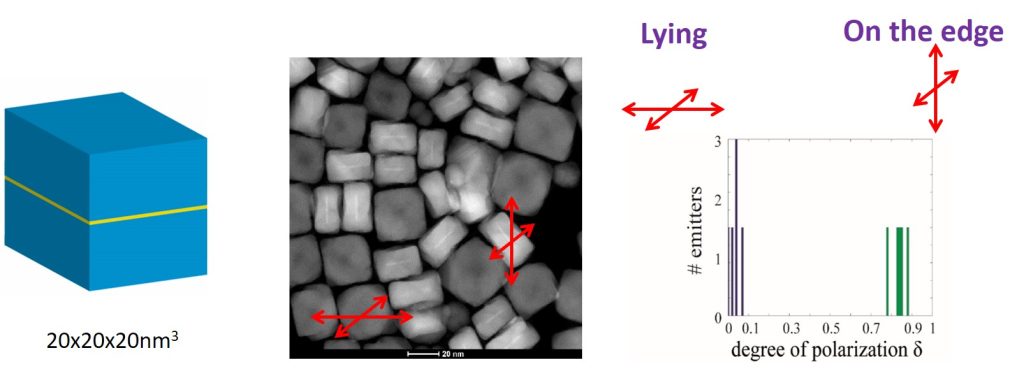
a) Nanocube. core: central layer of CdSe, surrounded by two thick layers of CdS. b) Electron microscopy image (@LPEM). Emission polarization statistics for 10 nanocubes. CdSe/CdS nanocubes can be deposited either on the edge or flat. From their emission polarization, their orientation can be detected.
- As part of an innovation program, we are also developing an instrument to characterize a large number of emitters simultaneously (in collaboration with Hugo Defienne).
Emission under strong excitation
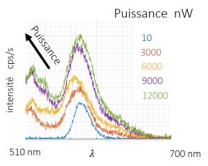
Under strong excitation, the spectrum of a single CdSe/CdS nanocrystal broadens.
At low laser excitation (less than 1 mW), the quantum box emits between the two fundamental levels of the electron and the hole. The nanocrystal can then be likened to a two-level system, emitting single photons centered on a line typically 20-30nm in spectral width. Under strong excitation, the behavior of the emitter changes completely, and the emission spectrum can reach 200nm in width. The two-level system is no longer a satisfactory model.
We have developed a new model for the emission of these nano-emitters, based on a statistical description of level occupancy. We have thus been able to define a temperature and a chemical potential of the carriers, which increase with excitation power.
Bayesian analysis
Processing our experimental data requires fitting a large number of parameters, some of which are correlated. Conventional methods of fitting by minimizing the deviation from a function are no longer appropriate. We have developed an original Bayesian analysis approach which has enabled us to determine the parameters specific to our experiments and validate our theoretical models.
Biological sensor
Using electron lithography, we fabricate dielectric disks and impregnate them with semiconductor nanocrystals. Gallery modes are excited by the fluorescence of the nanocrystals at the periphery of the disk, enabling the creation of an evanescent electric field in the immediate vicinity of the disk. Antigenes enable biological molecules of interest to be grafted onto both the disk and fluorophores. These are then placed in the field of the evanescent wave and fluoresce, enabling detection of the biological molecule.
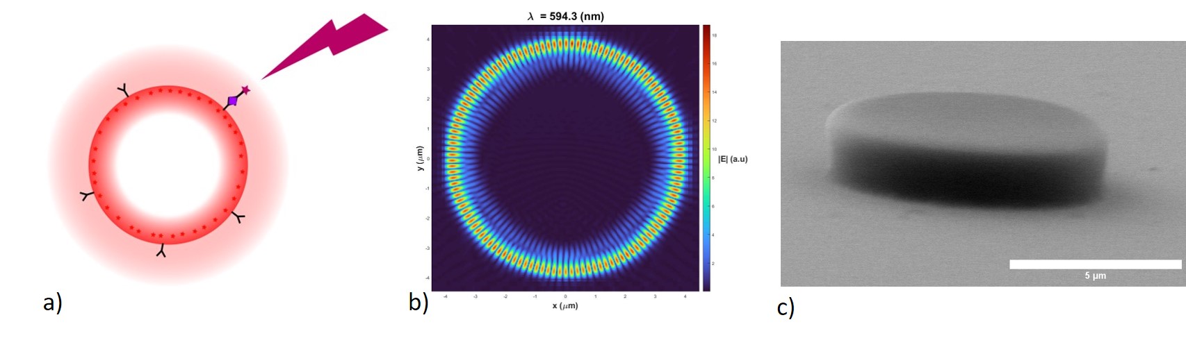
a) Principle of the biosensor. red dots: nanocrystals, purple diamonds: molecules of biological interest, red stars: fluorophores. b) gallery mode in the microdisk (FDTD simulation). c) electron microscopy image of the microdisk.
Plasmonic nano-antennas
An antenna is a device that enhances the coupling between a local electrical oscillator and a propagating electromagnetic wave. Antennas are widely used for transmitting and receiving radio waves, but their visible counterparts have only recently been considered because their dimensions must be controlled with precision below the wavelength scale. For us, the oscillator is a nano-emitter, a nanocrystal that interacts with a resonant electric field in the antenna.
The patch antenna consists of a gold substrate, covered by a thin layer of dielectric (10-50nm), the whole covered by a small gold disk, the patch, optically thin, from 500nm to 2 µm in diameter. In this antenna, a single nanocrystal is deterministically positioned at the center of the antenna. Positioning the light emitter within the antenna is a particularly delicate aspect. We have developed several lithography protocols, two of which are patented, for the deterministic positioning of a single nanocrystal at the center of a patch antenna.
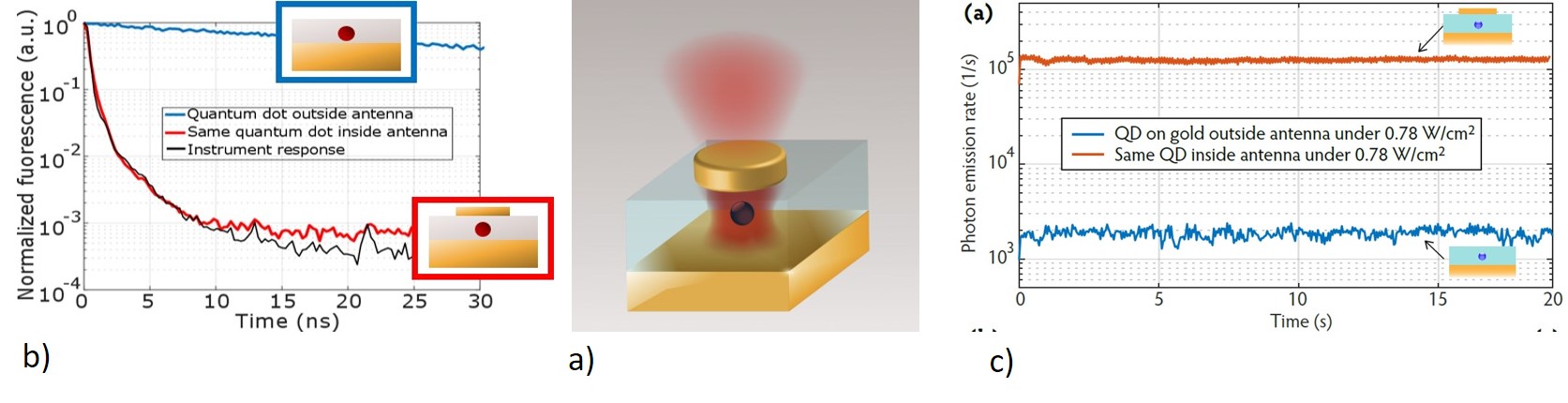
a) Scheme of a patch antenna; for the same emitter, before and after patch deposition, b) decay curve: fluorescence is accelerated by a factor >200 for the emitter in the antenna, c) fluorescence intensity. It is increased by a factor of 70 for the emitter in the antenna.
For this emitter, once inside the antenna, we have shown a strong acceleration of the lifetime, a strong improvement of the luminescence and an increase of 3 orders of magnitude of the absorption cross-section.
Collaborations
- Hugo Defienne (INSP, Nanopt team)
- Simon Huppert (INSP, Oxyde team)
- Thomas Pons at the ESPCI (Paris)
- Robson Ferreira (LPENS)
Publications
- C. Lethiec, J. Laverdant, H. Vallon, C. Javaux, J.-M. Frigerio, B. Dubertret, L. Coolen, A. Maître, Three-dimensional orientation measurement of a single fluorescent nanoemitter by polarization analysis, Phys. Rev. X 4, 021037 (2014),https://journals.aps.org/prx/pdf/10.1103/PhysRevX.4.021037
- F. Feng, L. Thu N’Guyen, M. Nasilowski, B. Nadal, B. Dubertret, L. Coolen, A. Maître, Consequence of shape elongation on emission asymmetry for colloidal CdSe/CdS nanoplatelets, nanoresearch 11, 3593 (2018), https://doi.org/10.1007/s12274-017-1926-3
- Feng, L. Thu NGuyen, M. Nasilowski, B. Nadal, B. Dubertret, A. Maître, L. Coolen,Probing the Fluorescence Dipoles of Single Cubic CdSe/CdS Nanoplatelets with Vertical or Horizontal Orientations, ACS Photonics, 5, 1994, (2018),https://pubs.acs.org/doi/pdf/10.1021/acsphotonics.7b01475
- A. R. Dhawan, C. Belacel, J. U. Esparza-Villa, M. Nasilowski, Z. Wang, C. Schwob, J.-P. Hugonin, L. Coolen, B. Dubertret, P. Senellart, A. Maître, Extreme multiexciton emission from deterministically assembled single emitter subwavelength plasmonic patch antennas, Light: science and application, 9, 33 (2020) , https://www.nature.com/articles/s41377-020-0269-0
- A. R. Dhawan, M. Nasilowski, Z. Wang, B. Dubertret, A. Maître, Efficient single-emitter plasmonic patch antenna fabrication by deterministic in situ optical lithography using spatially modulated light, Advanced materials 34, 2108120 (2022) https://doi.org/10.1002/adma.202108120