
Ferroelectrics and semiconductor nanocrystals bromance
In semiconductors physics the pn junction occupies a central place being the building block of device such as LEDs or photodiodes. Usually, the junction is obtained by doping semiconductors through implantation of extrinsic impurities. If this procedure is well established for bulk and thin film semiconductors, this is not the case for colloidal nanocrystals. Asa result, alternative strategies had to be developed to manufacture diodes. This may be obtained by coupling the active layers to carrier selective transport layer or using electrostatic gates. Members of the INSP’s Physical-chemistry team are proposing an approach that is more energy-efficient and less sensitive to surrounding noise, by coupling the active optical layer with a ferroelectric material.
Figure
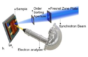
a. PFM (Piezoresponse force microscopy) image of the two ferroelectric domains written on the surface of the PZT. b. Schematic of the photoemission imaging measurement performed on the Antares de Soleil beamline relying on a X-ray nano-beam. C. Binding energy mapp for the 5d state of mercury on the area corresponding to the two ferroelectric domains from part a.
Reference
“Coupling Ferroelectric to colloidal Nanocrystals as a Generic Strategy to Engineer the Carrier Density Landscape”
Mariarosa Cavallo, Erwan Bossavit, Sylvia Matzen, Thomas Maroutian, Rodolphe Alchaar, Tung Huu Dang, Adrien Khalili, Corentin Dabard, Huichen Zhang, Yoann Prado, Claire Abadie, James K Utterback, Jean Francois Dayen, Mathieu G Silly, Pavel Dudin, Jose Avila, Emmanuel Lhuillier, Debora Pierucci
Advanced Functional Materials, 2300846 (2023)
pierucci(at)insp.jussieu.fr
This result is in cover of ACS Appl. Electron. Mater: