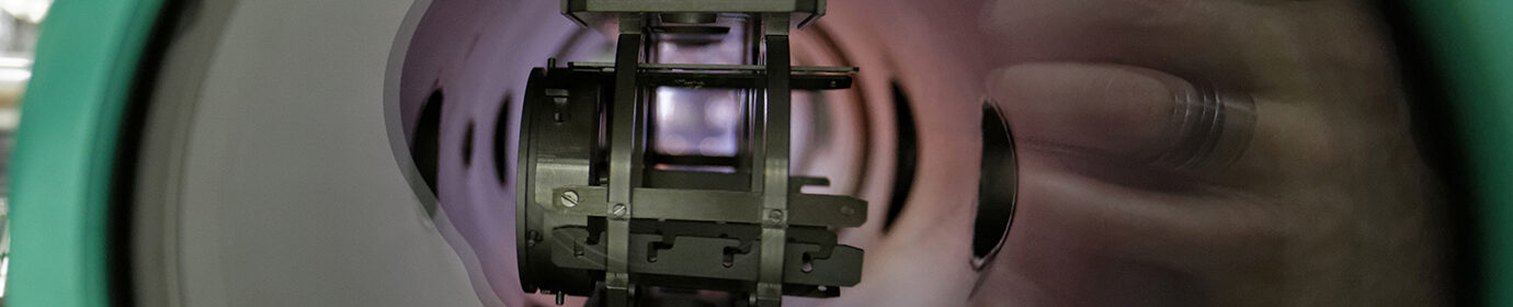


The Paris Institute of NanoSciences has a clean room. This structure opened its doors in October 2010. With its 170 m² of clean rooms, including 80 m² in ISO 6 cleanliness class (formerly class 1000, i.e. a certified controlled dust zone containing less than 1000 particles of 0.5 µm in diameter per foot3 of air) and 90 m² in ISO 7 class (class 10,000), this tool represents for the INSP an indispensable instrument in its research in the field of micro and nanotechnologies.
This micro-nano fabrication and characterization platform is an integral part of the consortium of clean rooms labeled “second circle Paris Centre” which includes five research entities: INSP, ENS, IPGG, Université Paris Cité (MPQ) and Observatoire de Paris.
This platform meets the needs of INSP members and is also open, upon request, to the scientific community and to companies.
The platform staff is in charge of welcoming and training users (researchers, PhD students, teachers, post-docs, students), advising and assisting researchers for the good realization of their scientific projects, maintaining and modernizing the equipment available, and enforcing the rules of use and safety inherent to such a facility.
This clean room allows the realization and characterization of micro and nanostructures specific to the different research fields developed within the INSP. Moreover, external projects can be hosted in this facility (for example, the realization of photolithography masks with the DWL).
Team
Erwan Dandeu, Mohamad Hamieh, Emmanuel Lhuillier
Contact
Direct line: 01 44 27 81 32
salleblanche(at)insp.jussieu.fr
Use the clean room
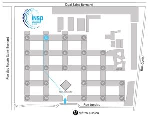
The entrance to the INSP clean room is located on the Jussieu campus, in the rotunda of tower 22, on the first floor (door 2223-SBC1, opposite the freight elevator).
| Access map |
 |
The keys allowing direct access to the clean room are held only by the persons in charge of this platform. The room is not self-service.
For any manipulation envisaged in the clean room, it is thus imperative to make a reservation on the GRR schedule set up for this purpose or to contact beforehand one of the persons in charge (Erwan Dandeu, Mohamad Hamieh, Emmanuel Lhuillier) in order to agree on an appointment.
For obvious organizational reasons, all reservations on the GRR schedule must be made at least 24 hours in advance at this address: http://www.insp.upmc.fr/grr
On the day of the appointment, a person in charge will be present to give you access to the room and guide you through your experiments. An intercom located at the entrance of the clean room allows you to signal your presence to the people already present inside.
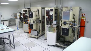
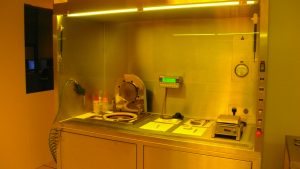
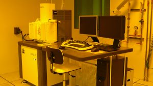
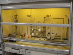
Equipment of the clean room
All the equipment necessary for basic manipulations is present on site. Ultra-pure water, as well as many acids, bases, solvents, resins, substrates and other consumables are available. However, for any particular request, please contact the persons in charge of the clean room.
Here are the main tools available to users:
| Deposition equipment | |
|
|
| Lithography equipment | |
 |
|
| Characterization equipment | |
|
|
| Various equipments | |
|
|
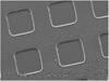
Examples of achievements
Here are some examples of samples realized at INSP thanks to the equipment present in the clean room.
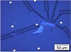
| Manufacture of photolithography masks | |
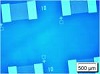 |
A l’aide de la technique de photolithographie à écriture directe par laser UV (DWL 66FS Heidelberg), des masques aux motifs variés peuvent être réalisés sur demande. Réalisation : Loïc Becerra, Mélanie Escudier |
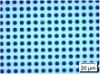
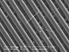
| Phononic crystals | |
 |
The modulation of acoustic properties at the scale of a hundred microns, at the origin of original behaviors, is obtained by etching holes in a silicon plate. Project author : Bernard Bonello |
 |
The modulation of acoustic properties at the micron scale is obtained by etching holes in a silica substrate.Project author : Laurent Belliard |
| Optical metamaterials | |
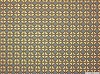 |
The structuring of thin films allows to obtain new physical properties of materials for their use in optics. Project author : Bruno Gallas |
| Multilayer deposition | |
 |
Structuring of a thick multilayer system in the form of dots (collaboration with the Femto-ST technology center in Besançon for the use of the DRIE technique). Project author : Bernard Bonello |
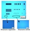
| Structuring of a GaMnAs thin film to obtain magnetic tracks or pads | |
 |
These structures allow the study of the structure and dynamics of magnetic domains, as well as the ultra-fast manipulation of magnetization. Project author : Laura Thevenard |
| Surface acoustic transducers | |
 |
Development of SAW type devices (inter-digitated emitter and receiver combs) for the study of magnetic thin films. Project author : Jean-Yves Duquesne |
| Isolated or interacting nanostructures | |
 |
The confinement of acoustic waves in nanostructured systems allows to highlight a discretization of the vibrational landscape. Project author : Laurent Belliard |
| Sensors | |
 |
A gold contact system is lithographed on the sample to be studied in order to extract by the 3ω method the conductivity of the underlying films. Project author : Jean-Yves Duquesne |
| Isolated or organized micron acoustic scatterers | |
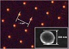 |
Under certain conditions, isolated nano and microstructures can interact with surface waves. Project author : Laurent Belliard |
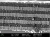
| Characterization of opal deposits by SEM | |
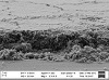 |
Project author : Agnès Maitre |
| Self-suspended systems | |
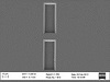 |
The realization of systems without interaction with the substrate is often an advantage in the study of their intrinsic properties. Project author : Laurent Belliard |
| Realization of electrodes | |
 |
After having located the sample to be studied on the surface of the substrate (here graphene), a system of electrodes was designed in order to perform transport measurements. Project author : Abhay Shukla (IMPMC) |
| Self-suspended copper nanowires on microstructured silicon substrate | |
 |
By photolithography and KOH wet etching, a Si substrate has been micro-structured. On the trenches, copper nanowires were then dispersed in order to study their vibrational properties. Project author : Laurent Belliard |
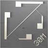
| Device for differential measurements of the speed of sound in liquids | |
|
In order to measure sound in liquid systems, differential measurements are very relevant. In this case, structures have been etched in a transparent substrate. Authors of the project : Laurent Belliard, Fréderic Decremps (IMPMC) |
Teatching
Person in charge: Laurent Belliard
Initiation to the different technologies related to the structuring of the material in clean room
Effects of rotation parameters during the coating of substrates, UV exposure parameters, development of positive or negative resins, chemical etching, anisotropic etching of silicon, lift-off process, thin film deposition, characterization techniques.
Teaching in the form of mini projects
The objective is to take advantage of the lithography processes in order to realize systems presenting functionalities that will have been introduced in the framework of more academic courses. The opening towards many UPMC training courses is under development (Research and Professional Masters, Internships) and should be amplified in the years to come.
Currently, two practical works, ranging from design to characterization of functional devices, are given in the clean room of the INSP: