List of members |
Facilities |
Internships and jobs |
PhD |
Publications |
News |
The common goal of the researches conducted within the team is the study of the correlation between the structure and the electronic and/or magnetic properties of semiconductor or insulating materials.
The systems of interest are involved in new devices for quantum technologies, information processing, and energy storage and conversion.
The team hosts both growth setup for the fabrication of these materials: ALD (Atomic Layer Deposition), PLD (Pulsed Laser Deposition) systems, together with powerful tools for analyzing their properties: electron paramagnetic resonance (EPR/FMR) spectrometers, advanced atomic force microscopes, and a Van de Graaff accelerator for ion beam analysis (SAFIR), which is developed and managed by the team.
The team has long been studying ultra thin dielectrics fims for microelectronic devices and has worked out both experimental and analytical methods to study the growth mechanisms, the interfaces and the defects of these nanometric films.
4 topics
| Materials for Energy storage | Materials for Energy conversion | Ferroic Memristors |
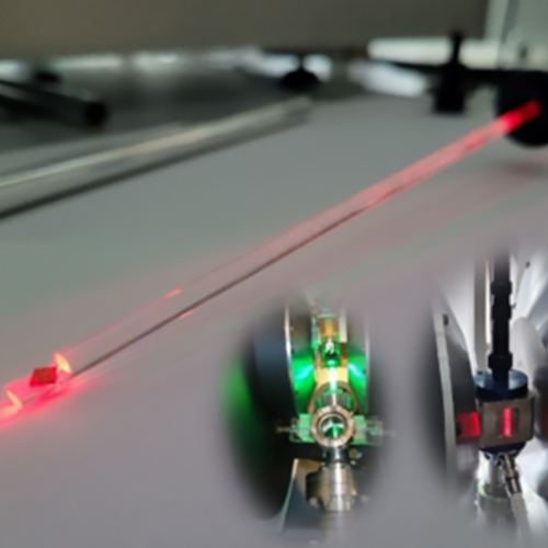
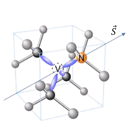
| Solid state Qubits |