Members
Emmanuel Lhuillier, Yoann Prado
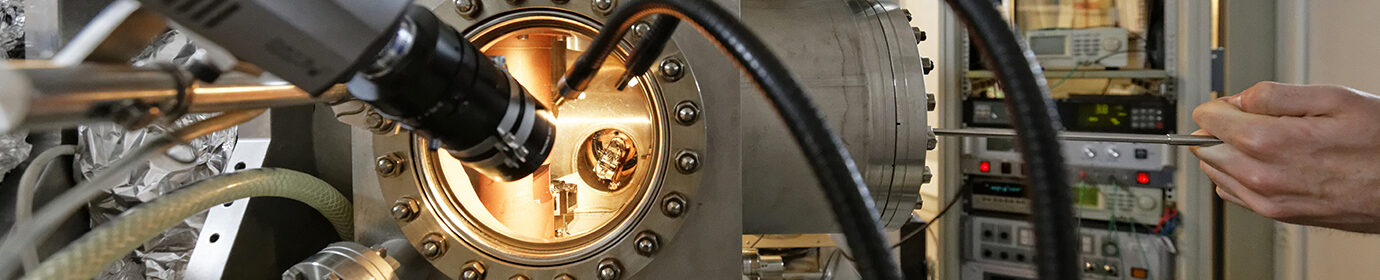
Nanocrystals are used as building blocks for optoelectronic components such as LEDs, solar cells, infrared detectors and cameras. This research activity has a clear focus on infrared materials, in particular PbS and HgTe nanocrystals, but we are also interested in perovskite materials or 2D materials (graphene, WSSe…). Our objectives are twofold: to correlate the electronic structure of confined semiconductors with their transport properties and to fabricate components in particular in the near and mid-infrared. The experimental techniques used are the following: nanoparticle synthesis and component fabrication using the INSP’s glovebox and clean room, absorption (200 nm to 150 µm) and emission (400 nm to 2.5 µm) spectroscopy, low-current electronic transport measurements, photoconduction measurements under cryogenic conditions, characterisation of optoelectronic components.
![]()
Figure: Emission of nanocrystals in the near infrared.
Doctoral students: C. Gréboval, A. Chu, A. Khalili, T. Dang
Defended theses: B. Martinez (2019), C. Livache (2019), J. Qu (2021)
Post-Doctoral students : S. Piereni, E. Izquierdo
Collaborations
- ESPCI – Sandrine Ithurria
- Synchrotron Soleil on Tempo (Mathieu Silly) and Smis (francesco Capitani) lines
- Onera – Greogory Vincent, New Imaging Technologies
Founding
- ERC BlackQD
- Project ANR-DGA NITQuantum
- ANR Copin and Frontal