Team
- Members : Jean-Louis Cantin, Ian Vickridge, Emrick Briand, Sébastien Steydli
- Emeritus researcher : Jurgen von Bardeleben
- PhD student: Thomas Ribault
Defects studies in wide band gap semiconductors
The energy transition requires the diversification of the sources of electrical energy and the optimization the grid to enable efficient energy distribution. As a result, there is a growing need for efficient power electronic devices that ensure voltage adaptation and conversion with minimal losses from these various sources to the end user.
Today, silicon-based power components are being replaced by higher-performance devices made from wide bandgap semiconductors such as silicon carbide (SiC) and gallium nitride (GaN).
Ultra-wide bandgap (UWBG) materials such as gallium oxide (Ga₂O₃), diamond, and aluminum nitride could further improve power transfer efficiency by enabling voltage conversions of several kilovolts and current intensities of several hundred amperes.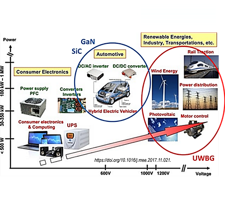
Caption: Applications of Ultra Wide Band Gap (UWBG) semiconductors for power devices
In this frame, gallium oxide has two main assets : its quite low cost and its very wide bandgap of 4.8 eV, which leads to an impressive breakdown field of around 8 MV/cm. While progress has been made in the growth of high-quality crystals, mastering the doping process and reducing electrically active defects, related to the crystal growth or induced by the device fabrication, remain critical steps. Indeed, these defects, located in the bulk or at interfaces, can act as recombination centers for charge carriers and thus modify the device performance.
The team has a long recognized expertise in the study of semiconductor defects using electron paramagnetic resonance (EPR). After contributing to overcoming technological barriers for the use of SiC in the microelectronics industry, we are now focusing on identifying defects in Ga₂O₃. Our research focuses on point defects such as vacancies, impurities or interstitial atoms, that generate electronic states in the bandgap and thus determine the electrical and optical properties of these materials, ultimately impacting device performance.
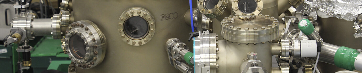
We use electron paramagnetic resonance to identify and quantify defects thanks to their electron spin. Our multi frequency electron magnetic resonance spectrometers allow for in situ optical excitation, providing insight into the energy level positions of these defects within the bandgap. We also make use of our ion accelerator (Safir) to generate defects through irradiation, in order to increase the defect concentration for analysis or understanding the degradation of components subjected to ion bombardment.
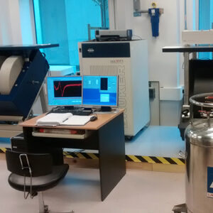
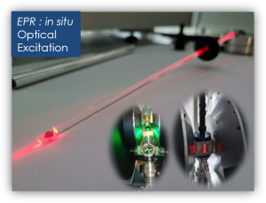
Caption: EPR set up. © INSP
This research is funded by :
– ANR – GOPOWER [2021-2025]: Accélérer la démonstration du potentiel de l’Oxyde de Gallium pour les applications du domaine de l’énergie. https://anr.fr/Projet-ANR-21-CE50-0015
– PEPR Electronique (Programmes et équipements prioritaires de recherche) – France 2030 – Projet GOTEN [2024-2028]: Repousser les limites de l’électronique de puissance : L’oxyde de gallium, le semi-conducteur de puissance de la prochaine génération. https://www.pepr-electronique.fr/goten/
![]()
Publications
- H. J. von Bardeleben, J. L. Cantin, High-Frequency Electron Paramagnetic Resonance and Electron-Nuclear Double Resonance Spectroscopy Study of the Ga Vacancy in β-Ga2O3, Physica Status Solidi B, 2400486 (2024)
- Unusual conduction mechanism of n-type β-Ga2O3: A shallow donor electron paramagnetic resonance analysis, Journal of Applied Physics 128, 125702 (2020) https://doi.org/10.1063/5.0023546
- JL Cantin, Magnetic resonance methods, Chapter 4 in ‘Characterisation and Control of Defects in Semiconductors’ p 151-198
Edited by Filip Tuomisto, Pub.: The Institution of Engineering and Technology
596 pages, ISBN : 9781785616556 (2019)