
Electron-electron repulsion and strong relativistic effects at the heart of the fundamental state properties of and a Pb atomic layer
In a metal, the direct repulsive interaction between two electrons (Coulombic interaction) is shielded by the presence of many other electrons. When the density of electrons decreases, this repulsive interaction between electrons increases. If this repulsion becomes strong enough, it can prevent the formation of a metallic state in favor of an insulating state called Mott insulator. Recent work has highlighted the amazing properties of these materials characterized by strong electronic correlations. Applications are currently being developed industrially, in particular for the fabrication of non-volatile memories, using both the metallic and insulating Mott states. From a theoretical point of view, modeling the electronic properties of these materials is a challenge due to the difficulty of modeling the strong interactions between electrons. This difficulty is even greater when it is a low dimensional system fabricated on a substrate: the role of the substrate atoms must also be considere.
In this context, researchers from the “Spectroscopy of Novel Quantum States” team have studied experimentally and theoretically a two-dimensional material consisting of a low-density lead atomic layer deposited on a silicon substrate. Predicted to be very close to the Mott transition, this system had never been studied at low temperature. Thanks to a fine comparison of the electronic excitation spectrum measured by STM with that calculated by an «ab initio» approach, the researchers showed that in this 2D material, the electronic correlations are not strong enough to induce an insulating state but significantly alter the metallic state. An important conclusion is also that the spin-orbite coupling, due to the high atomic mass of lead, is an essential parameter to be taken into account for the correct modeling of the electronic properties of this system which thus presents spin-polarized metallic states.
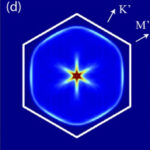
Caption: Calculation of these processes from the electronic structure obtained in DFT+U.
Reference
C. Tresca, C. Brun, T. Bilgeri, G. Menard, V. Cherkez, R. Federicci, D. Longo, F. Debontridder, M. D’Angelo, D. Roditchev, G. Profeta, M. Calandra and T. Cren, Chiral Spin Texture in the Charge-Density-Wave Phase of the Correlated Metallic Pb/Si(111) Monolayer, Phys. Rev. Lett. 120, 196402 (2018)
Partager ce contenu