Team
- Permanent members: Emmanuel Lhuillier, Yoann Prado, James Utterback
- PhD students: Charlie Gréboval, Audrey Chu, Adrien Khalili, Tung Dang Huu
- PhD defended: Bertille Martinez (2019), Clément Livache (2019), Junling Qu (2021)
- Post-Doctoral fellow: Stefano Piereni, Eva Izquierdo
The group is involved in the design of infrared optoelectronics devices using narrow band gap nanocrystals as active materials. This research topic is highly pluridisciplinar with:
- Nanocrystals synthesis, including the development of new growth method
- Device fabrication using clean room and air free processing in glove box
- Investigation of the material electronic structure
- Electronic transport with gate, temperature and time resolved possibilities
- Design of the light matter coupling to achieve high absorption and spectral shaping
- Integration of nanocrystals for the fabrication of infrared imaging system
- Infrared light emission
Collaborations
- ESPCI – Sandrine Ithurria
- Synchrotron Soleil, lignes Tempo (Mathieu Silly) et Smis (Francesco Capitani)
- Onera – Greogory Vincent
- New Imaging Technologies
Funding
- ERC BlackQD
- Project ANR-DGA NITQuantum
- ANR Copin and Frontal
Transversal topics
Nanocrystals synthesis, including the development of new growth method
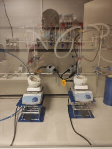
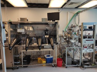
Caption: Image of nanocrystal synthetic setup.
For example, we report the first highly concentrated synthesis of HgTe nanocrystals by switching from conventional mercury salts to liquid mercury as precursor. We thus obtained the most concentrated synthesis of HgTe nanocrystal ever reported with concentration close to 100 g/L. This new synthetic route is promissing to achieve greener synthesis of HgTe with reduced exposure of work force to Hg precursor.
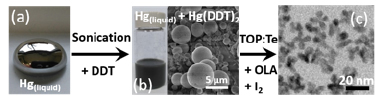
Caption: Scheme of liquid Hg based synthesis of HgTe nanocrystals.
We have also been the first to report nanocrystals with THz absorption. A new synthetic procedure has enable the growth of nanocrystal with size above the Borh radius, thus enabling absorption up to 100 µm. This work demonstrated the possibility to tune the absorption of HgTe nanocrystal all over the infrared from 1 to 100 µm.
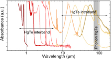
Caption: Infrared spectra of HgTe nanocrystals with various sizes.
Publications
- Nicolas Goubet, Maxime Thomas, Charlie Gréboval, Audrey Chu, Junling Qu, et al.. Near to Long-Wave Infrared Mercury Chalcogenide Nanocrystals from Liquid Mercury. Journal of Physical Chemistry C, American Chemical Society, 2020, ⟨10.1021/acs.jpcc.0c01255⟩. ⟨hal-02514168⟩
- Junling Qu, Nicolas Goubet, Clément Livache, Bertille Martinez, Dylan Amelot, et al.. Intraband Mid-Infrared Transitions in Ag 2 Se Nanocrystals: Potential and Limitations for Hgfree Low Cost Photodetection. Journal of Physical Chemistry C, American Chemical Society, 2018, ⟨10.1021/acs.jpcc.8b05699⟩. ⟨hal-01849301⟩
- Nicolas Goubet, Amardeep Jagtap, Clément Livache, Bertille Martinez, Hervé Portalès, et al.. Terahertz HgTe Nanocrystals: Beyond Confinement. Journal of the American Chemical Society, American Chemical Society, 2018, 140 (15), pp.5033-5036. ⟨10.1021/jacs.8b02039⟩. ⟨hal-01764916⟩
- Nicolas Goubet, Clément Livache, Bertille Martinez, Xiang Zhen Xu, Sandrine Ithurria, et al.. Wavefunction engineering in HgSe/HgTe colloidal heterostructures to enhance mid infrared photoconductive properties. Nano Letters, American Chemical Society, 2018, ⟨10.1021/acs.nanolett.8b01861⟩. ⟨hal-01807510⟩
Device fabrication using clean room and air free processing in glove box
We benefit from INSP clean room, as well as access to « Paris centre clean room consortium » giving us access to optical, laser and e-beam lithography. We also have possibilities to deposit metals and dielectrics including high-k materials. In the group, we also have gloved box for air free processing of the nanocrystal this include also an evaporator connected to the glove box for full air free fabrication of device.
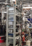
Caption: Image of setup for air free processing.
Investigation of the material electronic structure
Devices integration necessary requires a deep knowledge on the material electronic structure. Our main building block is HgTe nanocrystal which combine bulk inverted band structure with quantum confinement and surface chemistry dependence. It is thus of utmost importance to unveil band alignment of this material in absolute energy scale to be able to efficiently integrate it into devices with the right band alignment (low Schottky barrier).
To reach this goal, we use a combination of infrared spectroscopy and photoemission (mostly conducted on tempo beamline of synchrotron Soleil). We also use time-resolved photoemission which is a precious tool to probe carrier relaxation dynamics as well as surface band bending.
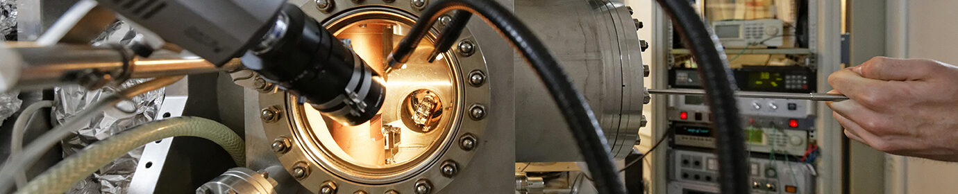
Caption: Photo of tempo beamline at Soleil.
Publications
- Clément Livache, Nicolas Goubet, Charlie Gréboval, Bertille Martinez, Julien Ramade, et al.. Effect of Pressure on Interband and Intraband Transition of Mercury Chalcogenides Quantum Dots. Journal of Physical Chemistry C, American Chemical Society, 2019, ⟨10.1021/acs.jpcc.9b01695⟩. ⟨hal-02120607⟩
- Dylan Amelot, Prachi Rastogi, Bertille Martinez, Charlie Gréboval, Clément Livache, et al.. Revealing the Band Structure of FAPI Quantum Dot Film and Its Interfaces with Electron and Hole Transport Layer Using Time Resolved Photoemission. Journal of Physical Chemistry C, American Chemical Society, 2020, 124 (6), pp.3873-3880. ⟨10.1021/acs.jpcc.9b10946⟩. ⟨hal-02514171⟩
- Amardeep Manikrao Jagtap, Bertille Martinez, Nicolas Goubet, Audrey Chu, Clément Livache, et al.. Design of Unipolar Barrier for Nanocrystal Based Short Wave Infrared Photodiode. ACS photonics, American Chemical Society,, 2018, ⟨10.1021/acsphotonics.8b01032⟩. ⟨hal-01908221⟩
- Clément Livache, Eva Izquierdo, Bertille Martinez, Marion Dufour, Debora Pierucci, et al.. Charge Dynamics and Optolectronic Properties in HgTe Colloidal Quantum Wells. Nano Letters, American Chemical Society, 2017, 17 (7), pp.4067-4074. ⟨10.1021/acs.nanolett.7b00683⟩. ⟨hal-01541341⟩
Electronic transport with gate, temperature and time resolved possibilities
Device performance directly relates to their transport properties. Investigation of the transport is thus a central topic in the group. We have develloped instrument to conduct measurement with Fermi level (ie with gate) and temperature witha resolution down to sub fA. We are also equipped to conduct photoconduction measurements (from UV to mid IR) with spectral and time resolved experiments. The instruments used to measured transport are not limited to nanocrystals fo HgTe and we also explore other materials such as TMDC, germanane, and other nanomaterials.
Publications
- Clément Livache, Bertille Martinez, Nicolas Goubet, Charlie Gréboval, Junling Qu, et al.. A colloidal quantum dot infrared photodetector and its use for intraband detection. Nature Communications, Nature Publishing Group, 2019, 10, pp.2125. ⟨10.1038/s41467-019-10170-8⟩. ⟨hal-02124021⟩
- Charlie Gréboval, Ulrich Noumbe, Nicolas Goubet, Clément Livache, Julien Ramade, et al.. Field effect transistor and photo transistor of narrow band gap nanocrystal arrays using ionic glasses. Nano Letters, American Chemical Society, 2019, 19 (6), pp.3981-3986. ⟨10.1021/acs.nanolett.9b01305⟩. ⟨hal-02122049⟩
- Charlie Gréboval, Audrey Chu, Debora Magalhaes, Julien Ramade, Junling Qu, et al.. Ferroelectric Gating of Narrow Band-Gap Nanocrystal Arrays with Enhanced Light Matter Coupling. ACS photonics, American Chemical Society,, 2021, 8 (1), pp.259-268. ⟨10.1021/acsphotonics.0c01464⟩. ⟨hal-03102784⟩
Design of the light matter coupling to achieve high absorption and spectral shaping
A central point in the design of infrared sensor using nanocrystal is the trade-off between absorption and carrier transport. Absorption pushed toward thick film (1 µm and more) but this is incompatible with the short carrier diffusion length resulting from hopping transport. By integrating plasmonic resonator, such as guided mode resonator, we are able to focus the light on a thin slab of semiconductor and achieve absorption close to unity. This strategy can also be used to design on demand absorption spectral or to offer spectral tunability beyond the material quantum confinement.
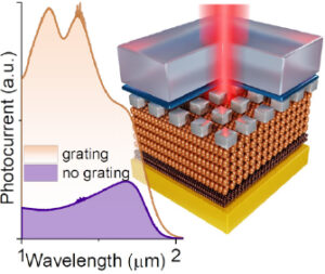
Caption: Left spectrum of a nanocrystal based sensor with and without a guided mode resonator to enhance its absorption. Right scheme of the device.
Publications
- Audrey Chu, Charlie Gréboval, Nicolas Goubet, Bertille Martinez, Clément Livache, et al.. Near Unity Absorption in Nanocrystal Based Short Wave Infrared Photodetectors using Guided Mode Resonators. ACS photonics, American Chemical Society,, 2019, ⟨10.1021/acsphotonics.9b01015⟩. ⟨hal-02281355⟩
- Prachi Rastogi, Audrey Chu, Charlie Gréboval, Junling Qu, Ulrich Nguétchuissi Noumbé, et al.. Pushing absorption of perovskite nanocrystals into the infrared. Nano Letters, American Chemical Society, 2020, 20 (5), pp.3999-4006. ⟨10.1021/acs.nanolett.0c01302⟩. ⟨hal-02542043⟩
- Prachi Rastogi, Audrey Chu, Tung Huu Dang, Yoann Prado, Charlie Gréboval, et al.. Complex Optical Index of HgTe Nanocrystal Infrared Thin Films and Its Use for Short Wave Infrared Photodiode Design. Advanced Optical Materials, Wiley, 2021, pp.2002066. ⟨10.1002/adom.202002066⟩. ⟨hal-03161581⟩
Integration of nanocrystals for the fabrication of infrared imaging system
Nanocrystals offer great promises as low-cost alternative to epitaxially grown infrared absorbing semiconductor. This is especially true in the short-wave infrared, where the cost of current sensor remains incompatible with many new infrared applications such as industrial vision. In collaboration with New Imaging Technologies, we design short wave infrared focal plane array where nanocrystals are used to functionalize a CMOS read out circuit to obtain short wave infrared photoconduction.

Caption: Image made with HgTe nanocrystals based sensor.
Publications
- Audrey Chu, Bertille Martinez, Simon Ferré, Vincent Noguier, Charlie Gréboval, et al.. HgTe Nanocrystals for SWIR Detection and their Integration up to Focal Plane Array. ACS Applied Materials & Interfaces, Washington, D.C. : American Chemical Society, 2019, ⟨10.1021/acsami.9b09954⟩. ⟨hal-02272333⟩
- Bertille Martinez, Julien Ramade, Clément Livache, Nicolas Goubet, Audrey Chu, et al.. HgTe Nanocrystal Inks for Extended Short‐Wave Infrared Detection. Advanced Optical Materials, Wiley, 2019, pp.1900348. ⟨10.1002/adom.201900348⟩. ⟨hal-02134751⟩
The group also works on light emission in geometrical LED geometry using nanocrystal as light emitter. Our interest goes beyond just the LED performance and we integrate LED for active imaging. In the infrared, the reflexion contrats can be quite different from the visible and this can be used for moisture detection for example, see the figure below.
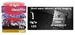
Caption: Left scheme of an infrared LED based on HgTe Nanocrystals. right scheme of a biscuit presenting a moisture strain that clearly appears under IR illumination while this stain presents no contrast in the visible.
Publications
- Junling Qu, Prachi Rastogi, Charlie Gréboval, Delphine Lagarde, Audrey Chu, et al.. Electroluminescence from HgTe Nanocrystals and its Use for Active Imaging. Nano Letters, American Chemical Society, 2020, ⟨10.1021/acs.nanolett.0c02557⟩. ⟨hal-02899117⟩
- Junling Qu, Prachi Rastogi, Charlie Gréboval, Clément Livache, Marion Dufour, et al.. A nanoplatelet-based light emitting diode and its use for all-nanocrystal LiFi-like communication. ACS Applied Materials & Interfaces, Washington, D.C. : American Chemical Society, 2020, ⟨10.1021/acsami.0c05264⟩. ⟨hal-02543986⟩
- Yoann Prado, Junling Qu, Charlie Gréboval, Corentin Dabard, Prachi Rastogi, et al.. Seeded growth of HgTe nanocrystals for shape control and their use in narrow infrared electroluminescence. Chemistry of Materials, American Chemical Society, 2021, ⟨10.1021/acs.chemmater.0c04526⟩. ⟨hal-03168405⟩