Where’s the bias, then?

Figure 1: Schematic of the operando X-ray photoemission measurement that enable the probing of the in plane and out plane electric field
In a device such as an LED, the applied electric field should be localized over the optically active layer, whereas the bias drop should be as limited as possible over the electrodes and charge transport layer that selectively brings carriers to the emitting layer. Therefore, being able to probe the spatial distribution of the electric field under operando conditions is critical. In a van der Waals heterostructure, two extreme cases can be investigated. When the resistivity of the two flakes is similar, the bias drop should be close to that of a homostructure, whereas when the conductivity of the flakes is different, for example when one flake is metallic, the latter should set its potential to a homogeneous value while the resistive flake accumulates the bias drop.
To be able to probe such energy maps, the group at INSP, in collaboration with colleagues from IMPMC, uses the facilities of the ANTARES beamline at Synchrotron Soleil. The sub-µm X-ray beam available on this line enables spatial resolved photoemission measurement (see Figure 1), allowing the tracking of the binding energy shifts across the device. Furthermore, because the spatial resolution of the map is high, we can even access the electric field orientation both in-plane (drain bias) and out-of-plane (gate bias).
L’équipe a appliqué cette méthode au cas d’une hétérostructure WS₂/MoSe₂. Cette dernière a d’abord été caractérisée par cartographie chimique. Pour cela, une carte Raman a été acquise à l’aide de la plateforme INSIDE de l’INSP (Figure 2a), permettant une localisation précise des deux feuillets. Ensuite, sur la ligne Antares, l’échantillon a été caractérisé sur la même zone ; pour chaque point, un spectre correspondant au W 4f (pour WS₂) et au Se 3d (pour MoSe₂) a été enregistré. Les chercheurs ont ensuite suivi le décalage de l’énergie de liaison lorsque les tensions de drain et de grille étaient appliquées (voir Figure 2b).
The team applied this method to the case of a WS₂/MoSe₂ heterostructure. The system was first characterized through chemical mapping. A Raman map was acquired using the INSIDE platform from INSP (Figure 2a), allowing precise localization and identification of the two flakes. Then, the same region was analyzed at ANTARES beamline, where photoemission spectra of W 4f (for WS₂) and Se 3d (for MoSe₂) core levels were collected at each point We then tracked how the binding energy shifts as drain and gate biases were applied (see Figure 2b). Some counterintuitive results have been observed. For example, even when the electrodes were fabricated in an area where the flake is homogeneous in thickness, the bias drop was found to be affected by thicker areas of the flake located away from the electrodes. Moreover, in the case of the WS₂/MoSe₂ heterostructure, the interface between the two flakes does not accumulate much of the bias drop, while Schottky barriers were clearly formed at the interface with the electrodes.
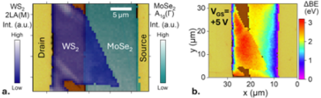
Figure 2 correlative microcopy imaging. a. Superimposed image of an optical microscopy and Raman chemical mapping obtained through the intensity of the 2LA mode of WS2 and A1g mode of MoSe2. b. Binding energy shift map induced by the application of 5 V of gate bias for the same device as in part a.
Researchers now aim to extend this study to the other extreme case, where the conductivity of the flakes strongly differs. This investigation will provide design guidelines for optimizing electrodes configurations, ensuring that the electric field is applied more effectively. Ultimately, the goal is to design devices with lower energy consumption and improved overall performance
Reference
Electric Field Distribution within a Van der Waals Heterostructure, D. Mastrippolito, M. Cavallo, E. Bossavit, C. Gureghian, A. Colle, T. Gemo, G. Strobbia, D. De Pesseroey, M. Paye, A. Khalili, H. Zhang, J. Biscaras, J. K Utterback, P. Dudin, J. Avila, E. Lhuillier, D. Pierucci, Nano Letters 25, 11340 (2025)
Contacts
- mastrippolito(at)insp.jussieu.fr
- pierucci(at)insp.upmc.fr