Quantum engineering of narrow band gap nanocrystals for Infrared optoelectronics
Contact : el@insp.upmc.fr
Tutelle : Sorbonne universite, INSP 4 place jussieu, 75005 Paris
Mots clés : Stage M2
Gratification : Oui
Page des stages de(s) l'équipe(s) : Physico-chimie et dynamique des surfaces
Description du stage
Click on « description » for full document
Keywords: Nanocrystals, device, LED, detector, synthesis.
Scientific description: Colloidal quantum dots are semiconductor nanoparticles, and their use as light sources for displays has been a breakthrough, leading to the 2023 Nobel Prize in Chemistry and opening a new billion-dollar market. While they have already reached commercial maturity in the visible range, their application in the infrared domain remains far less explored. However, this field is now attracting growing interest as a pathway toward more cost-effective optoelectronic devices.
Among the different candidate materials, we will focus on HgTe, which is the most spectrally tunable material, capable of covering the entire infrared range from the visible to the terahertz. The goal of the internship is to design and synthesize new core–shell nanostructures in order to control both the emission spectrum and the wavefunction localization.
The project has three main objectives: (i) Boost luminescence by at least one order of magnitude. (ii)Improve thermal stability of the nanocrystals and (iii) Maintain charge conduction, ensuring compatibility with LED and detector integration. This will be achieved through the careful selection of shell materials with optimized thickness and barrier height. The internship will also involve the integration of the nanocrystals into prototype devices dedicated to infrared light emission and detection, including fabrication and characterization steps.
This project offers the candidate an opportunity to acquire skills in nanomaterials synthesis, spectroscopy, and device physics, within a rapidly expanding research field at the interface between nanotechnology and optoelectronics.
References from the group
→ Photoconductive focal plane array based on HgTe quantum dots for fast and cost-effective short-wave infrared imaging, C. Gréboval et al, Nanoscale 14, 9359 (2022)
→Infrared Imaging using thermally stable HgTe/CdS nanocrystals, H. Zhang et al, Nano Lett 24, 5039 (2024)
→Electroluminescence from Nanocrystals above 2 μm, J. Qu et al, Nature Phot. 16, 38 (2022).
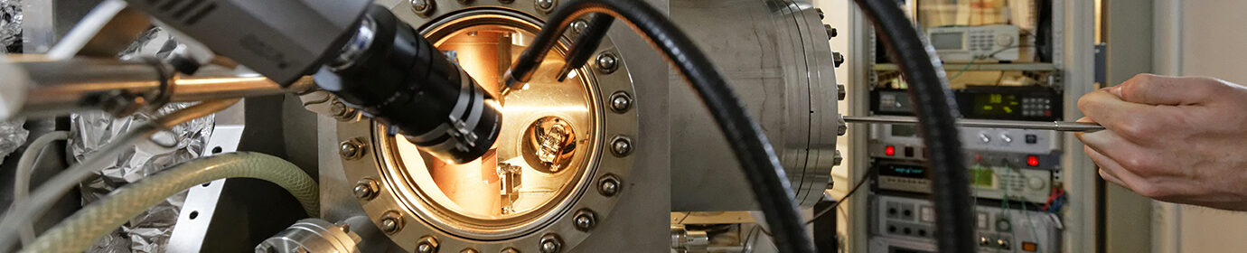
Techniques/methods in use: inorganic synthesis, clean room fabrication, characterization of material (IR spectroscopy, XPS) and device.
Applicant skills: Students must have a solid background in semiconductor physics and inorganic chemistry and be ready to work in an international environment (English as the daily working language, both written and spoken). Experience in clean room processes, nanocrystal-based devices, electronic transport, and instrument interfacing are also appreciated.