Infrared sensing with enhanced light matter coupling using quantum dot Scientific
Contact : el@insp.upmc.fr
Tutelle : Sorbonne universite, INSP 4 place jussieu, 75005 Paris
Mots clés : Stage M2
Gratification : Oui
Page des stages de(s) l'équipe(s) : Physico-chimie et dynamique des surfaces
Description du stage
Click on « description » for full document
Scientific project: Quantum dots, thanks to quantum confinement, offer an interesting playground for optoelectronics. In the visible range, they have already reached commercial status as light sources for displays, and current efforts now focus on the infrared range. Films of such colloidal quantum dots offer a strategy for cost disruption, while infrared optoelectronics has historically been prohibitive. However, their polycrystalline nature tends to limit carrier diffusion length; therefore, to efficiently absorb and photoconduct, they must be coupled to a photonic structure whose role is to focus light onto a thin film of such quantum dots. This concept is now established, and our group aims to go further through the introduction of post-fabrication reconfigurable structures, where the spectral response can be tuned via the application of a bias.
In this project, we aim to design new photonic structures that enable control of linewidth and absorption directivity. In the long term, the project could also shift toward light emission, depending on the applicant’s interests.
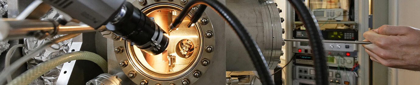
In practice, the intern will work on the design (electromagnetic simulations) of the photonic structures and will then fabricate the devices in the clean room and glove box, with support from chemists and clean room engineers. The intern will then characterize the devices, possibly at cryogenic temperatures, to demonstrate the benefits introduced by the cavity.
Students must have a solid background in semiconductor physics and be ready to work in an international environment (English as the daily working language, both written and spoken). Experience in clean room processes, nanocrystal-based devices, electronic transport, and instrument interfacing are also appreciated.
References from the group
→ Helmholtz Resonator Applied to Nanocrystal-based Infrared Sensing, C. Abadie et al., Nano Lett. 22, 8779 (2022)
→ Multiresonant Grating to Replace Transparent Conductive Oxide Electrode for Bias-Selected Filtering of Infrared Photoresponse, Tung H. Dang et al., Nano Lett. 23, 8539 (2023)
→ Stop Blaming Hopping Conduction in Nanocrystal Arrays, Use It for Active Photonics!, N. Ledos et al., Adv. Mater. Technol. 9, 2301463 (2024)
Methods and techniques: clean room fabrication, electromagnetic simulation, characterization of material (IR spectroscopy, XPS) and device (transport measurement, cryogenic condition)
Possibility to go on with a PhD ? yes and actually the applicant must be willing to continue PhD
Envisaged fellowship ? ANR or ERC already secured