Spatiotemporal Energy Transport in Advanced Energy Materials
Contact : james.utterback@insp.jussieu.fr
Tutelle : Institut des NanoSciences de Paris (INSP), Sorbonne Université and CNRS
Mots clés : Experimental et Stage M2
Gratification : Oui
Page des stages de(s) l'équipe(s) : Physico-chimie et dynamique des surfaces
Description du stage
CLIQUER SUR « Description du stage » pour avoir le document complet
Keywords: time-resolved spectroscopy, charge transport, nanocrystals, optoelectronics devices
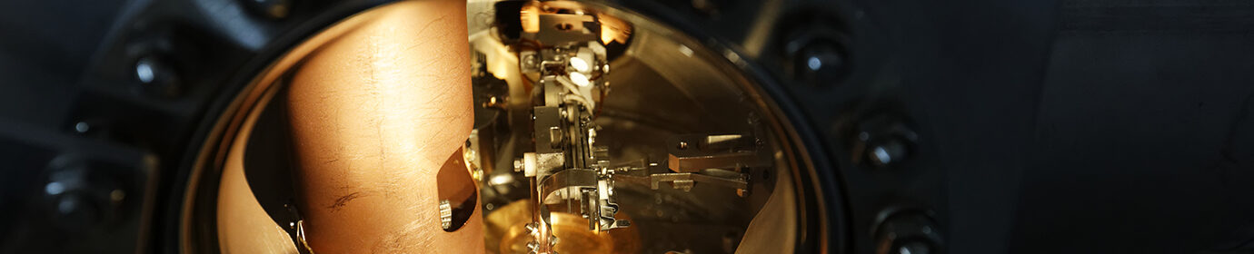
The aim of this project is to spatiotemporally study microscopic charge transport and dynamics in nanocrystal-based optoelectronics systems. Energy carrier transport across nanoscale interfaces is fundamental to the physical chemistry and functionality of energy conversion applications. While advanced spectroscopic methods grant an understanding of excited-state dynamics in isolated materials,1 many physical questions about the microscopic nature of transport in optoelectronics devices remain underexplored. To address this area, one needs a probe of local charge transport with sub-nanosecond time resolution and sub-micron spatial resolution in a material with realistic device conditions. Our approach is to do ultrafast microscopy and fabricate nanocrystal-based optoelectronics. These studies will reveal microscopic structure–property relationships that connect nanoscale carrier dynamics to macro-scale energy conversion.
During the timeframe of the master’s internship, the student will help to interface a pulsed white-light laser and spectrometer into an existing pump-probe microscopy setup, perform sample fabrication by lithography and self-assembly, and perform spectroscopy experiments. The goal is that the student continues on to do a PhD, during which the student will also use this state-of-the-art instrument to spatiotemporally measure the microscopic charge transport characteristics of advanced materials such as nanocrystal-based systems of interest.
The team: The student would be advised by Dr. James Utterback, a CNRS Chargé de Recherche at the Institut des NanoSciences de Paris (Sorbonne Université). Dr. James Utterback’s background is in pump-probe optical spectroscopy and microscopy of nanomaterials at the University of California Berkeley and University of Colorado Boulder.2 The student would also benefit from the environment of the Chemical Physics and Dynamics of Surfaces team, whose expertise spans across nanocrystal synthesis, characterization, spectroscopy, and nanocrystal device integration.
Student Background and Learning: The student will gain expertise in spectroscopy, clean room, data acquisition, data analysis and nanoscience. The student will develop data acquisition using LabView—a very commonly used program for data acquisition in physical chemistry labs. Scientifically, the student will study microscopic charge transport in next-generation semiconductor devices. Students with background in the above areas are preferred.
[1] Delor et al. Nature Materials, 2020, 19(1), 56. [2] Utterback et al. Nano Letters, 2021, 21(8), 3540.